
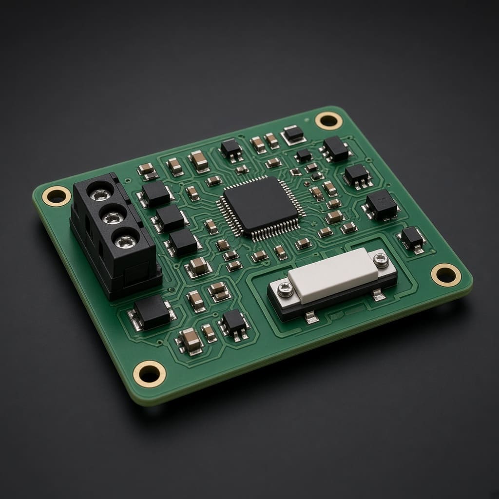
ADE9153 Single Channel AC Energy Metering
This blog contains Eagle schematic and PCB layout for ADE9153 test board
Based on the analysis of the schematic titled ADE9153A ENERGY METER V1.1, here is an updated and detailed version of the blog post, incorporating specifics from the actual circuit design:
Designing a Custom ADE9153A Energy Meter Evaluation Board – Schematic and PCB Overview
This article provides a technical walkthrough of a custom-designed energy meter evaluation board using Analog Devices’ ADE9153A IC. The schematic and PCB were developed in Autodesk Eagle, with the goal of creating a compact, accurate, and safe platform suitable for evaluating single-phase energy measurement systems.
IC Selection – ADE9153A
The ADE9153AACPZ serves as the core of the design. It supports accurate measurements of active, reactive, and apparent power, voltage, current, power factor, and line frequency. Integrated mSure® autocalibration ensures long-term accuracy without external calibration.
Key Sections of the Schematic
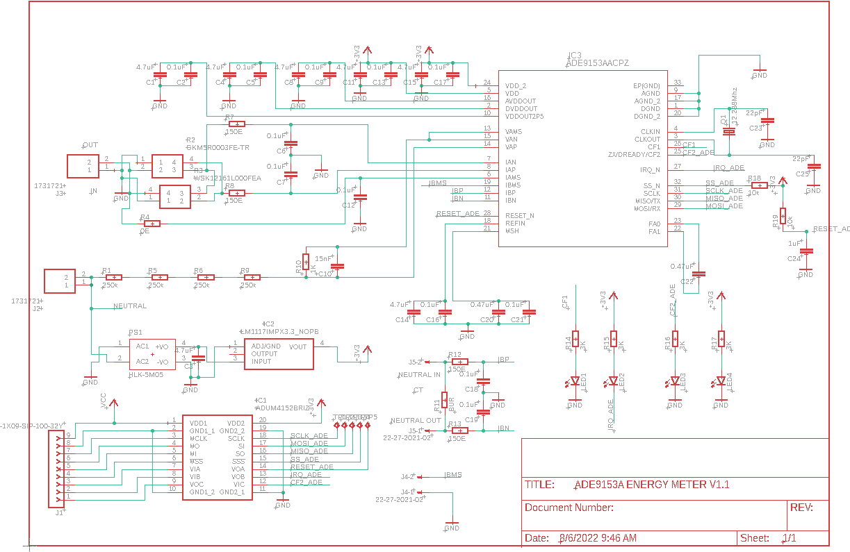
1. Voltage and Current Sensing
-
Voltage Sensing:
- Voltage is tapped from the AC input via a resistor divider using four high-value 250kΩ resistors in series.
- Additional RC filtering ensures signal stability before entering the ADE9153A’s voltage sensing pin (
VAP,VAN). - Safety and filtering are handled with multiple 0.1µF capacitors and 15nF ceramic caps.
-
Current Sensing:
- The design uses a WSK12161L000FEA precision shunt resistor.
- Inputs
IAP,IANare connected directly to the ADE9153A for current channel A, with low-noise analog filtering in place.
2. Power Supply and Regulation
- AC-DC conversion is handled by a HLK-5M05 module, which steps down mains AC to 5V DC.
- A LM1117IMPX-3.3 LDO regulator further regulates the 5V down to 3.3V, required for the ADE9153A and logic components.
- Bypass capacitors (4.7µF, 0.1µF, 1µF) ensure clean power rails.
3. Digital Isolation and Interface
- An ADUM4152BRIZ digital isolator provides SPI isolation between the metering IC and the external microcontroller interface.
- The SPI lines (
MOSI,MISO,SCLK,SS_N) and interrupt signals (IRQ_N,CF1,CF2) are all routed through the isolator. - Adequate test points are provided for SPI lines and control signals.
4. Clock Circuit
- The system uses a 8.288 MHz crystal oscillator with 22pF load capacitors to feed the
CLKINpin of ADE9153A. - The
CLKOUTpin is available for further timing use or debugging.
5. Headers and Debug Access
- J2, J3, J5 headers are provided for interfacing with an external MCU.
- Clearly labeled signals like
RESET_ADE,IRQ_ADE,MOSI_ADE,SCLK_ADEsimplify firmware development. - Test points (TP1–TP5) aid in probing key nodes during bring-up.
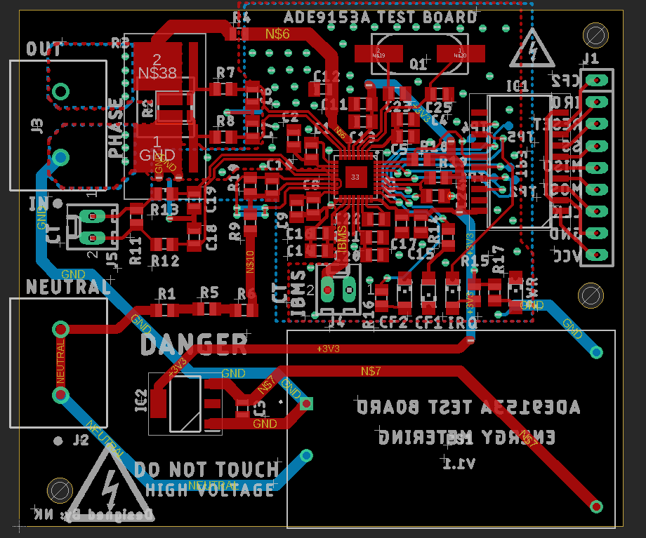
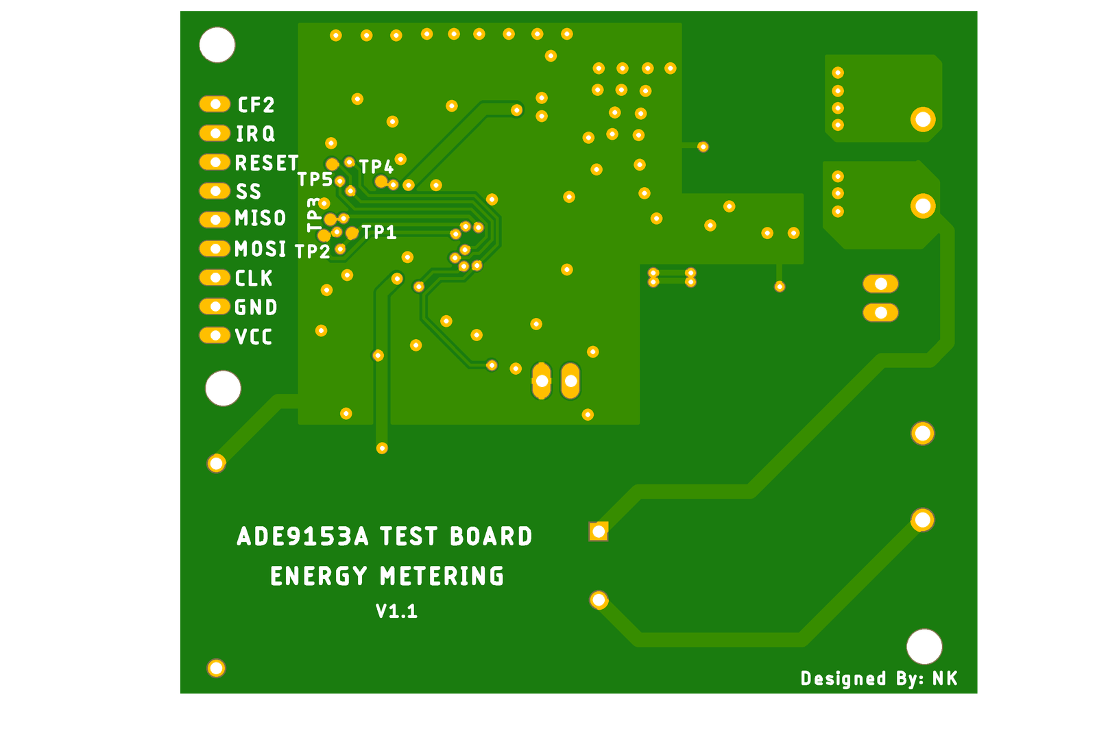
PCB
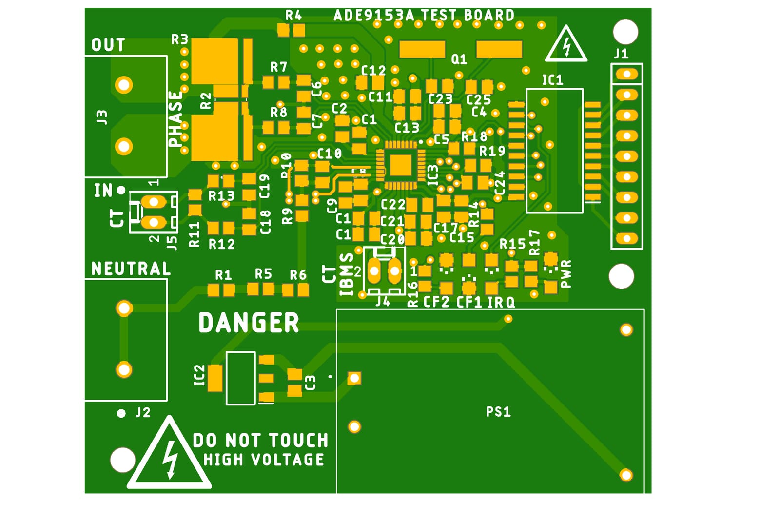
Safety and Layout Practices
- The schematic includes series 150Ω resistors and 0.1µF capacitors at several critical nodes to reduce high-frequency noise and protect against transients.
- High-voltage and low-voltage sides are physically isolated.
- Creepage and clearance are respected in PCB layout design to comply with safety norms for mains operation.
Referance
- Programming and Calibration details are here
- Evalution Board
Eagle Design Files
🔗 Design Files
Need this engineered for your product?
Tell us about your application — we’ll help with architecture, PCB, firmware, and production support.